A Charge-Pump PLL for On-Chip Clock Generation — 120 nm CMOS
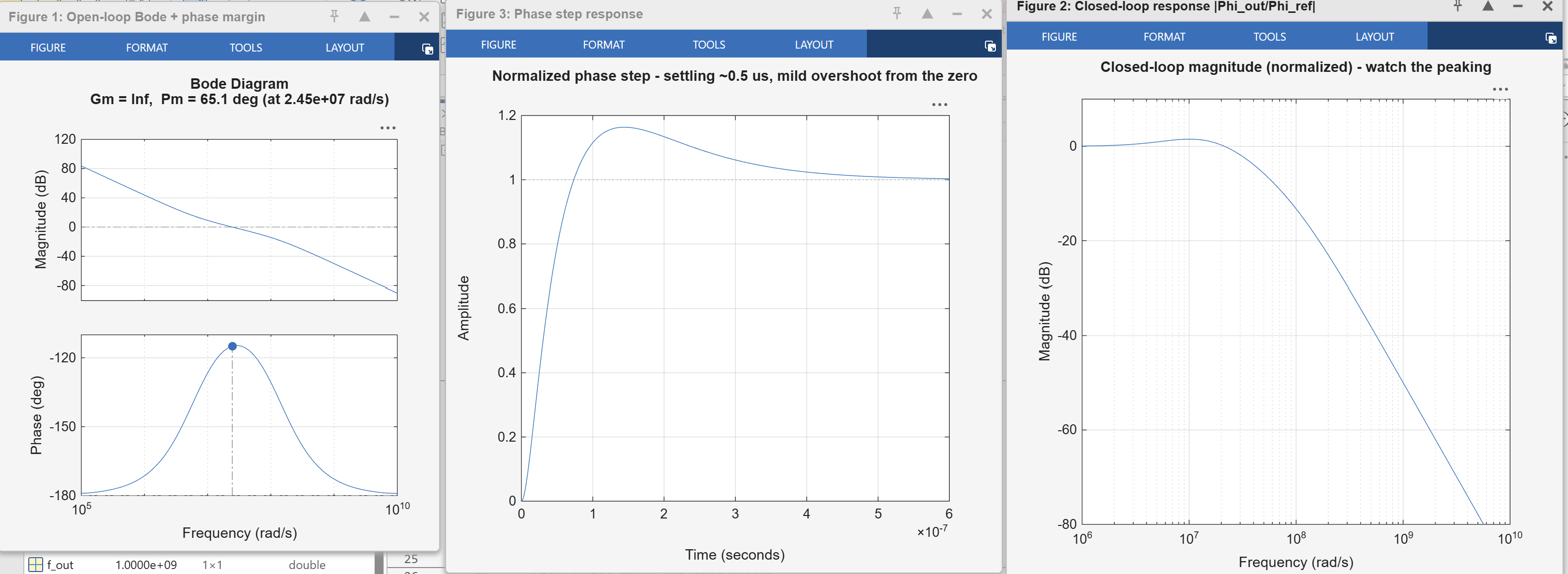
I'm designing an integer-N charge-pump PLL to synthesize low-jitter on-chip clocks for novel memristive-memory and compute-in-pixel sensor arrays, working alongside a PhD student in Duke's Roy Lab. The project runs the full mixed-signal flow: from a linearized loop model in MATLAB down to a transistor-level design in SkyWater's SKY120 (120 nm) process.
Target specs
| Parameter | Value |
|---|---|
| Architecture | Integer-N charge-pump PLL |
| Reference | 25 MHz |
| Output | 100–500 MHz (÷4 to ÷20) |
| Loop bandwidth | ~1 MHz (≈ f_ref / 25) |
| Damping factor (ζ) | ≈ 1 (~65° phase margin) |
| RMS jitter | < 5 ps |
| Process | SkyWater SKY120, 120 nm CMOS |
1. What a PLL Is
A phase-locked loop is a negative-feedback system that locks an oscillator's phase and frequency to a reference. Here it's used for frequency synthesis — multiplying a clean, slow reference up to a fast on-chip clock — the same way a car's cruise control holds a target speed by continuously correcting.
2. The Blocks — and How I Chose the Values
PLL design is mostly a control problem. I fix the two things that actually matter — loop bandwidth (~1 MHz) and damping (ζ ≈ 1) — then back-solve every component from the standard second-order loop equations. Loop bandwidth stays under f_ref / 20 so the loop behaves like a continuous-time system, and ζ ≈ 1 is the sweet spot between fast settling and low jitter peaking.
- Phase-Frequency Detector (PFD)Compares reference and divided-VCO edges and emits UP/DOWN pulses proportional to phase error. Edge-triggered, so input duty cycle is irrelevant. I add a reset delay to guarantee a minimum pulse width and kill the "dead-zone" around small phase errors.
- Charge Pump (I_cp ≈ 20 µA)Converts the PFD's digital pulses into an analog error current. I pick a mid-range I_cp to balance loop-filter capacitor area against noise, and use long-channel, cascoded current mirrors to match UP/DOWN currents (which keeps static phase error small).
- Loop Filter (C1 ≈ 100 pF, R ≈ few kΩ, C2 ≈ 5 pF)Sets the loop dynamics. C1 integrates the pump current and sets the natural frequency; R adds the stabilizing zero that gives ζ ≈ 1; C2 smooths charge-pump ripple on the control voltage. I keep C1/50 < C2 < C1/10 — small enough to preserve phase margin, large enough to cut ripple-induced jitter.
- Voltage-Controlled Oscillator (VCO)A current-starved ring oscillator whose frequency tracks the control voltage. Sized for a 100–500 MHz range with extra headroom for PVT spread; K_VCO falls out of the tuning range over the usable V_ctl window. Odd number of stages to guarantee oscillation, on a regulated supply to reject VDD noise.
- Feedback Divider (÷4 to ÷20)Sets the multiplication ratio. Implemented as a synchronous counter, clocked faster than the max VCO frequency to avoid run-away, with a re-sampling flop on the output to remove glitches before they reach the PFD.
3. Design Flow
I'm taking the design through four stages, each catching a different class of problem before the next:
- 01MATLABLinearized, frequency-domain model of the loop. Bode/phase-margin analysis locks in loop bandwidth and damping, then I solve for I_cp, C1, R, and C2.
- 02SimulinkTime-domain behavioral model of the whole loop. Verifies lock time, settling, and overshoot under a reference step and across frequency-range changes — before touching a transistor.
- 03KiCadA discrete, through-hole demo board (op-amp and logic-level parts) that proves the architecture and loop behavior cheaply on the bench.
- 04Cadence VirtuosoTransistor-level schematic and Spectre simulation of every block in the SKY120 PDK, swept across PVT corners for jitter and lock behavior.
4. Problems I Hit — and Fixed
A PLL has a lot of ways to fail. Three the loop model and transistor-level sims flagged, and how I'm designing around them:
VCO rails at power-on.
the VCO pins to its max frequency at start-up and outruns the divider.
the loop tries to lock before the supply is stable, saturating the control voltage to VDD.
hold the PLL in RESET until a power-OK signal asserts, keeping V_ctl at 0 until the rails settle.
Loop won't lock.
the PLL intermittently refuses to acquire lock.
glitches on the feedback-divider output confuse the PFD.
re-sample the divider output with a clean flop to strip glitches before they hit the phase detector.
Static offset from leaky capacitors.
the control voltage drifts and static phase error creeps up.
thin-gate-oxide capacitors leak badly at small nodes — a real concern at 120 nm.
build the loop-filter caps from thick-oxide / metal (MOM) capacitors. They cost more area, but the gate leakage that drives static phase error goes away.